- Home
- Research
- Education & Outreach
- Facilities
- Industry
Nano News & Events
How nanotechnology enables wearable electronics
Smart watches, fitness trackers, smart garments, smart medical attachments, data gloves - the market for wearable electronics is quickly evolving beyond health care, fitness and wellness into infotainment, and commercial and industrial applications. A review investigates the contribution of nanomaterials in the field of wearables with a focus on actuators and sensors. It discusses current applications of nanomaterials in this field and touch upon the different materials and methods being used.
Categories: Nanotechnology News
Apple, Huawei Both Claim First 7-nm Smartphone Chips
TSMC is the big winner, having made them bothAt an event today, Apple executives said that the new iPhone Xs and Xs Max will contain the first smartphone processor to be made using 7 nm manufacturing technology, the most advanced process node. Huawei made the same claim, to less fanfare, late last month and it’s unclear who really deserves the accolades. If anybody does, it’s TSMC, which manufactures both chips.
TSMC went into volume production with 7-nm tech in April, and rival Samsung is moving toward commercial 7-nm production later this year or in early 2019. GlobalFoundries recently abandoned its attempts to develop a 7 nm process, reasoning that the multibillion-dollar investment would never pay for itself. And Intel announced delays in its move to its next manufacturing technology, which it calls a 10-nm node but which may be equivalent to others’ 7-nm technology.
Apple’s new A12 Bionic is made up of six CPU cores, four GPU cores, and an 8-core “neural engine” to handle machine learning tasks. According to Apple, the neural engine can perform 5 trillion operations per second—an eight-fold boost—and consumes one-tenth the energy of its previous incarnation. Of the CPU cores, two are designed for performance and are 15 percent faster than their predecessors. The other four are built for efficiency, with a 50 percent improvement on that metric. The system can decide which combination of the three types of cores will run a task most efficiently.
Calling the A12 Bionic “an impressive feat,” VLSI Research analyst G. Dan Hutcheson says the chip “demonstrates that the attractiveness of staying on Moore’s Law has not diminished.”
Huawei’s chip, the Kirin 980, was unveiled at the IFA 2018 in Berlin on 31 August. It packs 6.9 billion transistors onto a one-square-centimeter chip. The company says it’s the first chip to use processors based on Arm’s Cortex-A76, which is 75 percent more powerful and 58 percent more efficient compared to its predecessors the A73 and A75. It has 8 cores, two big, high-performance ones based on the A76, two middle-performance ones that are also A76s, and four smaller, high-efficiency cores based on a Cortex-A55 design. The system runs on a variation of Arm’s big.LITTLE architecture, in which immediate, intensive workloads are handled by the big processors while sustained background tasks are the job of the little ones.
Kirin 980’s GPU component is called the Mali-G76, and it offers a 46 percent performance boost and a 178 percent efficiency improvement from the previous generation. The chip also has a dual-core neural processing unit that more than doubles the number of images it can recognize to 4,500 images per minute.
The Kirin 980 debuts in Huawei’s Mate 20 on 16 October. The first new generation iPhones start to ship on 21 September.
This post was corrected to show the right number of CPU cores and updated to include analyst comment and shipping dates.
Categories: Nanotechnology News
Grafoid Introduces a New Range of Oxidized Graphene Products, GNOX
Focus Graphite Inc. is happy to announce that Grafoid has launched a new series of oxidized graphene products called GNOX™ across the globe. Highly customizable graphene products are...
Categories: Nanotechnology News
GlobalFoundries Halts 7-Nanometer Chip Development
After installing extreme-ultraviolet lithography, foundry finds it doesn’t have enough customers for itIn a major shift in strategy, GlobalFoundries is halting its development of next-generation chipmaking processes. It had planned to move to the so-called 7-nm node, then begin to use extreme-ultraviolet lithography (EUV) to make that process cheaper. From there, it planned to develop even more advanced lithography that would allow for 5- and 3-nanometer nodes. Despite having installed at least one EUV machine at its Fab 8 facility in Malta, N.Y., all those plans are now on indefinite hold, the company announced Monday.
The move leaves only three companies reaching for the highest rungs of the Moore’s Law ladder: Intel, Samsung, and TSMC.
It’s a huge turnabout for GlobalFoundries. During a tour of Fab 8 last October, executives told IEEE Spectrum that 7-nm chips would be, at the very least, in limited production by the close of 2018. At the time, the company was completing installation of its first EUV lithography machine, a delicate and extremely expensive task.
GlobalFoundries rationale for the move is that there are not enough customers that need bleeding-edge 7-nm processes to make it profitable. “While the leading edge gets most of the headlines, fewer customers can afford the transition to 7 nm and finer geometries,” said Samuel Wang, research vice president at Gartner, in a GlobalFoundries press release.
“The vast majority of today’s fabless customers are looking to get more value out of each technology generation to leverage the substantial investments required to design into each technology node,” explained GlobalFoundries CEO Tom Caulfield in a press release. “Essentially, these nodes are transitioning to design platforms serving multiple waves of applications, giving each node greater longevity. This industry dynamic has resulted in fewer fabless clients designing into the outer limits of Moore’s Law. We are shifting our resources and focus by doubling down on our investments in differentiated technologies across our entire portfolio that are most relevant to our clients in growing market segments.”
(The dynamic Caulfield describes is something the U.S. Defense Advanced Research Agency is working to disrupt with its $1.5-billion Electronics Resurgence Initiative. Darpa’s partners are trying to collapse the cost of design and allow older process nodes to keep improving by using 3D technology.)
Specifically, GlobalFoundries is doubling down on chips made using it’s 14/12-nm FinFET process and plans to expand and develop the set of features offered at that node such as RF, embedded memory, low power, and other technologies. “Lifting the burden of investing at the leading edge will allow GF to make more targeted investments in technologies that really matter to the majority of chip designers in fast-growing markets such as RF, IoT, 5G, industrial, and automotive,” said Gartner’s Wang.
Pressing pause on advanced manufacturing nodes was a wise move because it will improve GlobalFoundries financial prospects, according to VLSI Research analyst G. Dan Hutcheson. “If you’re a customer your biggest question is not just the technology but financially stability,” he says. Foundries “really have to have a path to profitability.”
GlobalFoundries isn’t the only company struggling with its crawl further down the Moore’s Law rabbit hole. Recently, Intel revealed that it was delaying its move to a 10-nm process until 2019. (Intel’s 10-nm process is thought to be roughly equivalent to others’ 7-nm processes.) That puts a yawning five-year gap between manufacturing nodes for the company.
The delay has allowed TSMC, which began offering 7-nm this year, to pass Intel. AMD, once GlobalFoundries’ biggest processor customer, has already been working with TSMC on 7-nm chips and—in line with GlobalFoundries plans—announced that it will focus “the breadth” its 7-nm resources there going forward.
In a blog post Monday, AMD CTO Mark Papermaster wrote that the company’s first 7-nm GPU will come out later this year, and its first 7-nm server processor will launch in 2019. That would put AMD on a more advanced manufacturing node than Intel for the first time this century, notes ExtremeTech.
Of the remaining three bleeding-edge manufacturers, only TSMC doesn’t compete directly with at least some potential customers. “It puts TSMC in a very unique position, and I’m sure they’ll leverage that,” says VLSI’s Hutcheson.
The change at GlobalFoundries will involve layoffs among the staff at Malta. The number could be in the hundreds, according to The Albany Business Review.
This post was corrected on 18 September. Mark Papermaster is AMD’s CTO not it’s CEO. (That’s Lisa Su.)
Categories: Nanotechnology News
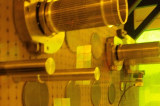
Researchers quickly harvest 2-D materials, bringing them closer to commercialization
Since the 2003 discovery of the single-atom-thick carbon material known as graphene, there has been significant interest in other types of 2-D materials as well.
These materials could be stacked together like Lego bricks to form a range of devices with different functions, including operating as semiconductors. In this way, they could be used to create ultra-thin, flexible, transparent and wearable electronic devices.
However, separating a bulk crystal material into 2-D flakes for use in electronics has proven difficult to do on a commercial scale.
The existing process, in which individual flakes are split off from the bulk crystals by repeatedly stamping the crystals onto an adhesive tape, is unreliable and time-consuming, requiring many hours to harvest enough material and form a device.
Now researchers in the Department of Mechanical Engineering at MIT have developed a technique to harvest 2-inch diameter wafers of 2-D material within just a few minutes. They can then be stacked together to form an electronic device within an hour.
The technique, which they describe in a paper published in the journal Science, could open up the possibility of commercializing electronic devices based on a variety of 2-D materials, according to Jeehwan Kim, an associate professor in the Department of Mechanical Engineering, who led the research.
The paper’s co-first authors were Sanghoon Bae, who was involved in flexible device fabrication, and Jaewoo Shim, who worked on the stacking of the 2-D material monolayers. Both are postdocs in Kim’s group.
The paper’s co-authors also included students and postdocs from within Kim’s group, as well as collaborators at Georgia Tech, the University of Texas, Yonsei University in South Korea, and the University of Virginia. Sang-Hoon Bae, Jaewoo Shim, Wei Kong, and Doyoon Lee in Kim’s research group equally contributed to this work.
“We have shown that we can do monolayer-by-monolayer isolation of 2-D materials at the wafer scale,” Kim says. “Secondly, we have demonstrated a way to easily stack up these wafer-scale monolayers of 2-D material.”
The researchers first grew a thick stack of 2-D material on top of a sapphire wafer. They then applied a 600-nanometer-thick nickel film to the top of the stack.
Since 2-D materials adhere much more strongly to nickel than to sapphire, lifting off this film allowed the researchers to separate the entire stack from the wafer.
What’s more, the adhesion between the nickel and the individual layers of 2-D material is also greater than that between each of the layers themselves.
As a result, when a second nickel film was then added to the bottom of the stack, the researchers were able to peel off individual, single-atom thick monolayers of 2-D material.
That is because peeling off the first nickel film generates cracks in the material that propagate right through to the bottom of the stack, Kim says.
Once the first monolayer collected by the nickel film has been transferred to a substrate, the process can be repeated for each layer.
“We use very simple mechanics, and by using this controlled crack propagation concept we are able to isolate monolayer 2-D material at the wafer scale,” he says.
The universal technique can be used with a range of different 2-D materials, including hexagonal boron nitride, tungsten disulfide, and molybdenum disulfide.
In this way it can be used to produce different types of monolayer 2-D materials, such as semiconductors, metals, and insulators, which can then be stacked together to form the 2-D heterostructures needed for an electronic device.
“If you fabricate electronic and photonic devices using 2-D materials, the devices will be just a few monolayers thick,” Kim says. “They will be extremely flexible, and can be stamped on to anything,” he says.
The process is fast and low-cost, making it suitable for commercial operations, he adds.
The researchers have also demonstrated the technique by successfully fabricating arrays of field-effect transistors at the wafer scale, with a thickness of just a few atoms.
“The work has a lot of potential to bring 2-D materials and their heterostructures towards real-world applications,” says Philip Kim, a professor of physics at Harvard University, who was not involved in the research.
The researchers are now planning to apply the technique to develop a range of electronic devices, including a nonvolatile memory array and flexible devices that can be worn on the skin.
They are also interested in applying the technique to develop devices for use in the “internet of things,” Kim says.
“All you need to do is grow these thick 2-D materials, then isolate them in monolayers and stack them up. So it is extremely cheap — much cheaper than the existing semiconductor process. This means it will bring laboratory-level 2-D materials into manufacturing for commercialization,” Kim says.
“That makes it perfect for IoT networks, because if you were to use conventional semiconductors for the sensing systems it would be expensive.”
Categories: Nanotechnology News
Nano: a cleaner option?
Could nanotechnology tidy up the planet without leaving a dangerous residue of its own?It's likely that you've recently swirled nanotechnology down your sink. Antimicrobial silver nanoparticles, for example, are added to food containers, socks, and cleaning products such as floor polish. But could nanoparticles – measuring less than 100 nanometres wide – clean more than just your house? Could nanotechnology tidy up the planet without leaving a dangerous residue of its own?The European Environment Agency estimates that "potentially polluting activities" have occurred at nearly three million EU sites. But nanoparticles could remediate water, soil and air polluted by compounds such as heavy metals and aromatic hydrocarbons. With high reactivity and a larger surface area than the same mass of material in a larger form, nanoparticles are prime candidates for capturing and destroying pollutants. Continue reading...
Categories: Nanotechnology News