- Home
- Research
- Education & Outreach
- Facilities
- Industry
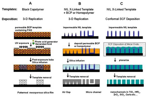
Test Bed 2: Hierarchical Metal Oxide Films
Well defined, patterned metal oxide films are essential device layers in a broad range of applications including microelectronics, photovoltaics, microfluidics, separations and sensors. The ability to control structure and function at the nanoscale, as well as the device scale, will lead to tremendous advancements in capability. Examples include: (1) continued scaling of interconnect structures in integrated circuits, (2) fabrication of high density arrays of high aspect ratio capacitors for information processing, memory elements and energy storage, (3) complex channel structures for microfluidics, and (4) fabrication of semiconductor (titania) electrodes for photovoltaic devices. Current limitations include both the cost and resolution limits of top-down fabrication methods. In a typical process sequence a planar metal oxide film is deposited, coated with multi-layer resist structures, patterned by optical lithography, etched, stripped, ashed and cleaned to generate a patterned oxide film. This cycle often consists of 10 or more process cycles. Moreover, the resolution of current lithography and etch techniques limit minimum feature size to greater than 30 nm and prevent the direct fabrication of complex geometric structures. In this test bed, we take advantage of four of the CHM’s core technologies (ordered BCP templates, 3-D replication, NIL, conformal SCF deposition) to provide a uniquely capable tool kit for the rapid and cost effective preparation of hierarchical metal oxides, in which structure is generated and controlled simultaneously at both the nanoscale and the device levels and the need for pattern etching in the oxide is eliminated. The approaches yield both cost and performance advantages, as many target structures cannot be accessed through other means. The strategies are shown in Figure 7.29. The challenges for theses approaches include the development of photopatternable templates based on chemically amplified resist technology to improve device level pattern resolution, the development of novel NIL resists that exhibit the chemical and thermal compatibility requirements necessary to achieve the process strategies articulated in the process flow, the chemical functionalization and modification of the resulting oxide structures to achieve performance metrics and demonstration of full wafer process scaling.