- Home
- Research
- Education & Outreach
- Facilities
- Industry
Nanomanufacturing Process Research
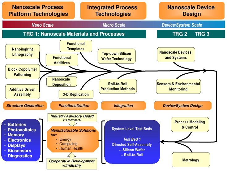
Figure 1: Vision and Systems-Level Organization
The Center for Hierarchical Manufacturing (CHM) is a leading research and education center for the development of precision and cost efficient process platforms and tools for the manufacturing of next generation, nanotechnology-enabled devices for electronics, energy conversion, resource conservation and human health. The Center’s approach involves the integration of components and systems across multiple length scales and integrates nanofabrication processes for sub-30 nm elements based on directed self-assembly, additive-driven assembly, nanoimprint lithography, and conformal deposition at the nanoscale with Si wafer technologies or high-rate roll-to-roll based production tools. The CHM effort is made comprehensive by research on device design, modeling and prototype testing in functional architectures that take advantage of the specific hierarchical nanomanufacturing capabilities developed by the Center.
The implementation of efficient nanomanufacturing strategies that are compatible with Si wafer processing or high-volume roll-to-roll processing will enable the production of high performance computing, memory, sensing and photonic/optically active media and devices as well as nanoenabled products in energy conversion, organic electronics and displays at acceptable cost. Such advances will help to transform the nation’s substantial investment in basic research into products that provide substantial societal and economic benefits.
Fundamental and Translational Research: The CHM research structure consists of three Technical Research Groups (TRGs), (1) Nanoscale Materials and Processes, (2) Nanoscale Devices, Systems, and Metrology and (3) Sensors and Environmental Monitoring, in which fundamental research is performed. Translational research is conducted in the system-level test beds in which the key science, engineering and process barriers to the manufacturing of device nanostructures using the CHM platform tools are identified, systematically addressed and resolved. The CHM’s fundamental science and translational test bed efforts incorporate faculty and research professionals at UMass Amherst, MIT, The University of Michigan, Mount Holyoke College, NIST, The University of Puerto Rico, and Rice University and benefit from collaborations with leading groups in Europe and Asia.
Technical Research Groups: The three Technical Research Groups, which involve more than thirty investigators at UMass Amherst and our collaborating institutions, are:
Research Highlights: Significant developments within the CHM to date include:
- Additive driven assembly for R2R preparation of ordered hybrid device layers: CHM researchers demonstrated through strong specific interactions, highly-ordered periodic templates could be obtained from blends of commercially-available commodity materials. Further, specifically functionalized metal and semiconductor nanoparticles can be used to drive strong order, enabling high loadings in hybrid materials. Together these enable low cost, roll-to-roll assembly of nanostructured media using self-assembly strategies.
- Floating gate memory via self-assembly: CHM investigators have used additive driven self-assembly to create the active device layer for floating gate memory. This approach, which allows for very high loadings of 2 nm gold nanoparticles in a polystyrene-block-poly(vinyl pyridine) block copolymer, offers theoretical storage capacities competitive with current flash memory devices. To achieve high storage densities in devices, device level patterning at micron and smaller length scales is required. We are currently pursuing the device patterning via roll-to-roll (R2R) nanoimprint lithography. These technologies will enable the production of memory and other devices using low cost, sustainable, nanomanufacturing.
- Roll-to-Roll Nanoimprint Lithography: The center accepted delivery of the first custom roll-to-roll nanoimprint lithography (R2RNIL) tool in June 2011. A similarly advanced R2R coater for nanostructured hybrid materials will be delivered early in 2012. Center researchers are now routinely printing sub-200 nm features in a continuous web process. Center researchers are currently developing new materials and processes to enable printing of features to the ten's of nanometers. Understanding flow and rheological properties is critical to the mission. Real-time inspection and metrology capabilities are being developed for the new tools.
- Patterned magnetic media from block copolymers: In the area of directed self-assembly, CHM research demonstrated reductions in feature size and attainment of long-range order necessary to generate templates for 10 terabyte/in2 media, an order of magnitude greater than previously possible.
- Biologically produced nanowires: CHM investigators contributed new research in which nanowires are grown naturally rather than synthesized chemically. This discovery may lead to new methods for biologically-produced or biologically-inspired materials for sustainable nanomanufacturing. Pilin nanofilaments (pili), known now as "microbial nanowires", are a class of fibrous proteins found in the sediment bacteria Geobacter. Temperature-dependent studies show the filaments possess metal-like characteristics. The conductivity can be modulated by doping, or by using an applied voltage in an electrochemical transistor configuration. Supercapacitor-level energy storage has been demonstrated with these materials.
- Nanoelectronics: The Center demonstrated a prototype of a multistate data storage element using a cluster of 3 interacting nanomagnets and a feasible route to manufacturing using guided self-assembly of block copolymers. In addition, plasmonic arrays were developed to demonstrate significantly enhanced fluorescence for sensor applications.
- Chemical nose sensors for rapid cancer diagnosis: The CHM developed a sensor array containing non-covalent gold nanoparticle-fluorescent polymer conjugates that is capable of detecting, identifying, and quantifying protein targets. CHM researchers also developed unique “chemical nose” sensors for cells and serum. These sensors target the rapid and efficient identification of healthy, cancerous, and metastatic cells for cancer diagnosis. CHM research further demonstrated that simple chemical functionalization of polycarbonate membranes generates effective tools for protein separations.
- Self-priming microfluidic biosensor: CHM researchers have developed a new format of biosensor based on self-priming microfluidics that will allow for a smaller and more sensitive biosensor, as well as commercial-scale manufacturing and low materials cost. It incorporates the simplicity and reliability of a lateral flow assay with a microfluidic device thanks to the development of a single-step surface modification method which allows strong capillary flow within a sealed microchannel.
- Formation of hierarchical ULK device structures: The CHM demonstrated the direct patterning of mesoporous films for use as ultra-low dielectric constant thin films in microelectronics using a process in which selective area exposure of block copolymer templates, doped with photoacid generators. simultaneously dictate structure at the nanoscale and device scales, achieving process efficiencies by eliminating the need for etching. The Center further developed techniques for producing nanochannel arrays that will enable modular design of on-chip devices for bio-molecule separations, sensors and diagnostics and a novel low cost spray-on approach of nanostructured metal oxide films for use in alternative energy generation.
- Easy Soft Imprint Nano-Lithography (ESINL) Process: The CHM demonstrated a new nanoimprint molding technique to rapidly prototype device structures and created nanowires of cadmium selenide (CdSe) using a simple electrochemical deposition process and polymer templates created by NIL. CHM researchers have developed an ESINL process to use polydimethylsiloxane rubber to replicate device patterns. It was used to fabricate organic field effect transistors. This represents the first use of soft imprint lithography to fabricate such devices.
- Biodistribution of nanoparticles: CHM scientists developed a new technique based on laser desorption/ionization mass spectrometry (LDI-MS) to track the distribution and fate of nanoparticles (NPs) in the environment. NPs with positively charged surfaces were found to be 3 to 10 times more likely to accumulate in fish than negative or neutral NPs. These results may inform the development of more environmentally sustainable nanomaterials for inclusion into commercial products, a result that is important to the CHM and to the broader nanomanufacturing community.
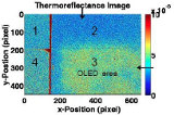
- Spin-offs: Alenas Imaging, Inc. was co-founded by CHM Participant Professor Janice Hudgings of Mount Holyoke College to commercialize the applications of stochastic resonance enhanced thermoreflectance (SRETR). This inspection method offers high spatial resolution and low cost for a wide range of nanomanufacturing applications. Alenas received a Phase I STTR grant from NSF to explore applications in the green energy industry.