- Home
- Research
- Education & Outreach
- Facilities
- Industry
Nano News & Events
Benefits of Metal Oxide Nanomaterials in Engineering Flexible and Wearable Sensors
The novel research published in the journal ACS Nanoscience focuses on a thorough examination of parameters that might increase the responsiveness of MON-based detectors in environmental aspects...
Categories: Nanotechnology News
Development of a single-process platform for the manufacture of graphene quantum dots
Precisely controls the bonding configuration of heteroatoms in graphene quantum dots through simple chemical processes. Practical application and commercialization in various fields is expected, including non-metallic catalyst materials.
Categories: Nanotechnology News
High-performance anode for all-solid-state Li batteries is made of Si nanoparticles
Large volume expansion during charging, the obstacle to using Si anodes in conventional liquid electrolytes, helps a Si anode composed of nanoparticles in solid electrolytes has high-rate discharge capability approaching those of Si films.
Categories: Nanotechnology News
Smart systems for semiconductor manufacturing
Integrating smart systems into manufacturing offers the potential to transform many industries. Lam Research, a founding member of the MIT.nano Consortium and a longtime member of the Microsystems Technology Lab (MTL) Microsystems Industrial Group, explored the challenges and opportunities smart systems bring to the semiconductor industry at its annual technical symposium, held at MIT in October.
Co-hosted by MIT.nano and the MTL, the two-day event brought together Lam’s global technical staff, academic collaborators, and industry leaders with MIT faculty, students, and researchers to focus on software and hardware needed for smart manufacturing and process controls.
Tim Archer, president and CEO of Lam Research, kicked off the first day, noting that “the semiconductor industry is more impactful to people's lives than ever before."
“We stand at an innovation inflection point where smart systems will transform the way we work and live,” says Rick Gottscho, executive vice president and chief technology officer of Lam Research. “The event inspires us to make the impossible possible, through learning about exciting research opportunities that drive innovation, fostering collaboration between industry and academia to discover best-in-class solutions together, and engaging researchers and students in our industry. For all of us to realize the opportunities of smart systems, we have to embrace challenges, disrupt conventions, and collaborate.”
The symposium featured speakers from MIT and Lam Research, as well as the University of California at Berkeley, Tsinghua University in Beijing, Stanford University, Winbond Electronics Corporation, Harting Technology Group, and GlobalFoundries, among others. Professors, corporate leaders, and MIT students came together over discussions of machine learning, micro- and nanofabrication, big data — and how it all relates to the semiconductor industry.
“The most effective way to deliver innovative and lasting solutions is to combine our skills with others, working here on the MIT campus and beyond,” says Vladimir Bulović, faculty director of MIT.nano and the Fariborz Maseeh Chair in Emerging Technology. “The strength of this event was not only the fantastic mix of expertise and perspectives convened by Lam and MIT, but also the variety of opportunities it created for networking and connection.”
Tung-Yi Chan, president of Winbond Electronics, a specialty memory integrated circuit company, set the stage on day one with his opening keynote, “Be a ‘Hidden Champion’ in the Fast-Changing Semiconductor Industry.” The second day’s keynote, given by Ron Sampson, senior vice president and general manager of US Fab Operations at GlobalFoundries, continued the momentum, addressing the concept that smart manufacturing is key to the future for semiconductors.
“We all marvel at the seemingly superhuman capabilities that AI systems have recently demonstrated in areas of image classification, natural language processing, and autonomous navigation,” says Jesús del Alamo, professor of electrical engineering and computer science and former faculty director of MTL. “The symposium discussed the potential for smart tools to transform semiconductor manufacturing. This is a terrific topic for exploration in collaboration between semiconductor equipment makers and universities.”
A series of plenary talks took place over the course of the symposium:
“Equipment Intelligence: Fact or Fiction” – Rick Gottscho, executive vice president and chief technology officer at Lam Research
“Machine Learning for Manufacturing: Opportunities and Challenges” – Duane Boning, the Clarence J. LeBel Professor in Electrical Engineering at MIT
“Learning-based Diagnosis and Control for Nonequilibrium Plasmas” – Ali Mesbah, assistant professor of chemical and biomolecular engineering at the University of California at Berkeley
“Reconfigurable Computing and AI Chips” – Shouyi Yin, professor and vice director of the Institute of Microelectronics at Tsinghua University
“Moore’s Law Meets Industry 4.0” – Costas Spanos, professor at UC Berkeley
“Monitoring Microfabrication Equipment and Processes Enabled by Machine Learning and Non-contacting Utility Voltage and Current Measurements” – Jeffrey H. Lang, the Vitesse Professor of Electrical Engineering at MIT, and Vivek R. Dave, director of technology at Harting, Inc. of North America
“Big and Streaming Data in the Smart Factory” – Brian Anthony, associate director of MIT.nano and principal research scientist in the Institute of Medical Engineering and Sciences (IMES) and the Department of Mechanical Engineering at MIT
Both days also included panel discussions. The first featured leaders in global development of smarter semiconductors: Tim Archer of Lam Research; Anantha Chandrakasan of MIT; Tung-Yi Chan of Winbond; Ron Sampson of GlobalFoundries; and Shaojun Wei of Tsinghua University. The second panel brought together faculty to talk about “graduating to smart systems”: Anette “Peko” Hosoi of MIT; Krishna Saraswat of Stanford University; Huaqiang Wu of Tsinghua University; and Costas Spanos of UC Berkeley.
Opportunities specifically for startups and students to interact with industry and academic leaders capped off each day of the symposium. Eleven companies competed in a startup pitch session at the end of the first day, nine of which are associated with the MIT Startup Exchange — a program that promotes collaboration between MIT-connected startups and industry. Secure AI Labs, whose work focuses on easier data sharing while preserving data privacy, was deemed the winner by a panel of six venture capitalists. The startup received a convertible note investment provided by Lam Capital. HyperLight, a silicon photonics startup, and Southie Autonomy, a robotics startup, received honorable mentions, coming in second and third place, respectively.
Day two concluded with a student poster session. Graduate students from MIT and Tsinghua University delivered 90-second pitches about their cutting-edge research in the areas of materials and devices, manufacturing and processing, and machine learning and modeling. The winner of the lightning pitch session was MIT’s Christian Lau for his work on a modern microprocessor built from complementary carbon nanotube transistors.
The Lam Research Technical Symposium takes place annually and rotates locations between academic collaborators, MIT, Stanford University, Tsinghua University, UC Berkeley, and Lam’s headquarters in Fremont, California. The 2020 symposium will be held at UC Berkeley next fall.
Categories: Nanotechnology News
Seminar: Nanofabrication for lithium metal batteries and perovskite solar cells - WSU News
Seminar: Nanofabrication for lithium metal batteries and perovskite solar cells WSU News
Categories: Nanotechnology News
Researchers Build New Database that Removes the Guesswork from Nanofiber Fabrication Process
Electrospinning is a nanofiber fabrication method that is capable of producing micrometer- to nanometer-diameter metallic, ceramic, and polymer fibers of numerous compositions for a broad spectrum of...
Categories: Nanotechnology News
Grafoid Launches Grafprint3D, New Company to Focus on Graphene 3D Printing
Grafoid has announced the worldwide launch of Grafprint3D (GP3D) Inc., a new company with a portfolio of products and solutions to focus on the worldwide additive manufacturing and 3D printing market...
Categories: Nanotechnology News
Nanotechnology and Advanced Materials Progress Under Horizon 2020 and Beyond
Future and innovation through nanotechnology at EuroNanoForum 2019, the most important European forum of the industry, in Bucharest The National Institute for Research and Development in...
Categories: Nanotechnology News
Rice Scientists Present Their Protocol for Carbon Nanotube Handling
With some practice, it would take just about 10 minutes, few bags, and a big bucket to maintain nanomaterials in their place. Chemist Andrew Barron from the Rice University lab works with bulk...
Categories: Nanotechnology News
First Graphene Secures Major Production Order for Mining Wear Linings
First Graphene has signed a new agreement with newGen for the supply of three tonnes of its PureGRAPH products. These will be used by newGen for the manufacture of wear linings used in bucket...
Categories: Nanotechnology News
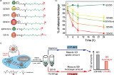
Graphene-based Wearable Health Trackers
Researchers at the ICFO (Institut de Ciencies Fotoniques) and the ICREA (Institució Catalana de Recerça i Estudis Avançats) in Barcelona have developed wearable fitness trackers based...
Categories: Nanotechnology News
Developed greener method based on MW implementation in manufacturing CNFs
Developed greener method based on MW implementation in manufacturing CNFsLoai Aljerf; Rim NadraInternational Journal of Nanomanufacturing, Vol. 15, No. 3 (2019) pp. 269 - 289This study comes as the first trial that uses microwave (MW) in combination with assisted chemical vapour deposition (CVD) to generate homogeneous carbon nanofibers (CNFs) at short period thermal reaction. The outcomes confirmed that these materials are of highly-ordered pyrolitic graphite nature. CNFs were obtained having uniform diameters (80-150 nm) and long fibres (0.82-1.75 μm). SEM and TEM evaluations revealed relatively less damage in fractured surfaces and the TGA exhibited insignificant change of CNFs during thermal decomposition. The 'solid' CNFs showed clear properties as disorder, crystalline, and bent graphitic sheets. The as-prepared CNTs demonstrated good MW-absorption properties with superior performance which could be due to the combination of the dielectric-type absorption and the interference of multi-reflected MW. This enhancement gave 97% purity of the novel manufactured CNFs. Therefore, we recommend our greener nanoproducts for industries as energy, pharmaceutical, cosmetics, textile, sensors, electronics, vehicles, and both of quantum dots (QD) and fluorescent C-dots.
Categories: Nanotechnology News
Minister Bains announces investment that will position Canada as global leader in nanomanufacturing - Canada NewsWire
Minister Bains announces investment that will position Canada as global leader in nanomanufacturing Canada NewsWire
Categories: Nanotechnology News
Pattern-transfer nanomanufacturing for micro-optics and spectroscopy - Laser Focus World
Pattern-transfer nanomanufacturing for micro-optics and spectroscopy Laser Focus World
Categories: Nanotechnology News
Heng Pan receives NSF CAREER award to advance nanomanufacturing research - Missouri S&T News and Research
Heng Pan receives NSF CAREER award to advance nanomanufacturing research Missouri S&T News and Research
Categories: Nanotechnology News
Large-scale synthesis of metal nanoclusters with thermal shocks
Researchers report significant advances in developing a high-temperature, fast nanomanufacturing technique for the large-scale production of ultra small metal nanoclusters decorated in a graphene host matrix. The size and morphology of the metal nanoclusters can be controlled by varying the reaction temperature and the mass loading of metal salt in the graphene aerosol nanoreactors. This one-step continuous aerosol-based thermal shock technique offers considerable potential for the manufacturing of well-dispersed and uniform nanoclusters stabilized within a host matrix.
Categories: Nanotechnology News
Roll to Roll Technologies for Flexible Devices Market to be at Forefront by 2023 - Market Industry Reports
Roll to Roll Technologies for Flexible Devices Market to be at Forefront by 2023 Market Industry ReportsRoll-to-roll processing, also referred to as web processing, reel-to-reel processing, or simply R2R, is the process of building electronic devices on a roll of ...
Categories: Nanotechnology News
IBM Pushes Beyond 7 Nanometers, Uses Graphene to Place Nanomaterials on Wafers
The functionality of devices could be changed simply by changing nanomaterials without impacting the processFour years ago, IBM announced that it was investing US $3 billion over the next five years into the future of nanoelectronics with a broad project it dubbed “7nm and Beyond.” With at least one major chipmaker, GlobalFoundries, hitting the wall at the 7-nm node, IBM is forging ahead, using graphene to deposit nanomaterials in predefined locations without chemical contamination.
In research described in the journal Nature Communications, the IBM researchers for the first time electrified graphene so that it helps to deposit nanomaterials with 97% accuracy.
“As this method works for a wide variety of nanomaterials, we envision integrated devices with functionalities that represent the unique physical properties of the nanomaterial,” said Mathias Steiner, manager at IBM Research-Brazil. “We also can envision on-chip light detectors and emitters operating within a distinct wavelength range determined by the optical properties of the nanomaterial.”
As an example, Steiner explained that if you wanted to modify the spectral performance of an optoelectronic device, you could simply replace the nanomaterial while keeping the manufacturing process flow the same. If you take the method one step further, you could assemble different nanomaterials in different places doing multiple passes of assembly to create on-chip light detectors operating in different detection windows at the same time.
The entire method can be considered a hybrid bottom-up/top-down process flow, according to Michael Engel, research staff member at IBM Research–Brazil. A couple of years ago, IBM created one of these hybrid processes that combined top-down manufacturing techniques—like lithography—with bottom-up techniques that “grow” electronics through self-assembly.
Engel explained that the first step of this hybrid process involves growing graphene directly on top of the substrate where the nanomaterial assembly is performed.
In IBM’s demonstration, they used graphene on silicon carbide. Engel noted that it is also possible to grow the graphene on another material, such as copper, then peel the graphene off and put it on a silicon/silicon oxide wafer.
The next step was etching the graphene to define the deposition sites. This is done at a large scale and can be considered the top-down part of the process.
The third step employs a bottom-up technique where researchers apply an AC electric field to the patterned graphene layers while depositing nanomaterial solution on top. The nanomaterial is then dragged down and trapped between opposing graphene electrodes.
“So the graphene fulfills the function of defining the placement location and providing the electric field orientation and drag force for the directed nanomaterial assembly,” said Engel.
In the fourth step of this process, the graphene deposition electrodes are etched away, followed by additional manufacturing steps for integrating and operating electronic or optoelectronic devices.
The state of the art prior to this work was using metal electrodes, which are difficult to remove and limit device performance and integration potential.
“We believe the biggest breakthrough of this work is the bottom-up placement of a wide variety of nanomaterials with nanometer-scale resolution over much larger, millimeter-scale areas with easily removable (residual free) electrodes,” said Steiner. “The graphene electrodes provide excellent nanomaterial alignment and density, limit chemical exposure, and avoid metal lines, enabling superior device performance.”
This process is not going to come to the rescue of Moore’s Law overnight. One of the biggest challenges, according to Engel, is introducing solution-based nanomaterials into the industrial-scale manufacturing process.
“This will require progress in the standardization of nanomaterial solutions to achieve repeatable and consistent results, as well as the adaption of the electric-field-assisted method for use in the wafer scale manufacturing processes,” said Engel.
While standardization of nanomaterial solutions is not going to be solved by IBM, the researchers are continuing to work on the device level of the technology with the integration of different nanomaterials in order to customize basic integrated circuits such as, for example, electrical inverters or ring oscillators.
Along these lines, the researchers are developing dedicated on-chip light emitters and detectors with spectral properties determined by the assembled nanomaterial.
Editor’s Note: A small change was made on October 9th to correct the mistaken description that the graphene was peeled off of silicon carbide and put onto a silicon/silicon oxide wafer. These are actually two different embodiments of the method: either graphene is grown on silicon carbide (where it stays in place for further processing), or the graphene is grown on copper and transferred to the wafer for further processing.
Categories: Nanotechnology News
Graphene Printing Technique "Silk Screens" Flexible Electronics
Graphene-based remote epitaxy enables inexpensive copying of gallium arsenide and gallium nitride chipsFuture high-efficiency solar cells molded to the surface of a car, ultrasmall photonics chips, and low-power, long-lasting wearable devices will all require something no one’s yet been able to achieve, namely chips made from high-efficiency materials that are flexible, thin, and inexpensive to manufacture.
A research group at MIT has announced a couple of developments in recent weeks that bring such a confluence of innovations closer to the achievable. Jeehwan Kim’s research group announced separately this month in Nature Materials and Science that they can inexpensively mass-produce ultrathin gallium arsenide and gallium nitride chips as well as harvest the monolayer materials necessary for manufacturing other 2D electronics, like tiny photonics devices.
“We [found] the way to go to expensive semiconducting materials so you can keep producing high-quality, high-performance semiconductors with a cheaper price,” says Kim, associate professor of mechanical engineering and materials science at MIT. “The bonus is, you can have flexible semiconducting devices, and because they’re really thin, you can stack them up.”
As IEEE Spectrum reported last year, Kim’s group essentially uses graphene sheets as nanosize silk screens through which expensively manufactured exotic-material-based semiconductors can be laid down.
The recipe: Take a costly, manufactured, ultrathin film of pure semiconducting material like gallium arsenide and lay a single-layered sheet of graphene on top of it. Then flow atoms of gallium and arsenide over the graphene, and the intermediary sheet acts as a surface on which an identical copy of the underlying ultrathin film is copied on top of the graphene— although how and why the process worked as well as it did had previously been unclear.
In the current work, Kim’s group has expanded and generalized their previous finding—discovering, on one hand, single-atom crystals like silicon cannot be replicated by the “silk screen” technique (what the group calls remote epitaxy) but on the other hand that practically any 2D sheet or film whose molecules carry any net electric polarity to them can be mass-produced via remote epitaxy.
The reason, the group discovered, is that electrically the graphene behaves as if it’s not even there, transmitting the ionic electric fields from the 2D material up to the slurry of raw materials resting on top of the graphene. The fields then guide the slurry into forming a perfect duplicate of the expensively manufactured thin film below.
Kim uses the shorthand term “copy-paste” to describe the simple and seemingly inexpensive procedure as it’s now being developed. (He admits, however, he cannot give price quotes at the moment, because they haven’t yet done an economic analysis of the process.)
“We were able to copy-paste…through graphene for many types of compound materials in the periodic table,” says Kim. “That is a big discovery. Based on that understanding, we were able to make single-crystalline, freestanding, very, very thin membrane compound materials.”
Kim says his research group is working with “six major companies” in Korea, Japan, and the United States to scale up the ultrathin chip manufacturing processes they’re developing. He expects some of these technologies might only need “a couple years” before they’re potentially ready for commercial application.
The industries and product lines Kim says could find use for the remote epitaxy process include solar energy (cheap but ultra-efficient GaAs solar panels have long been a dream), photonics (layering multiple ultrathin films on top of each other, say, so that each are efficient at transmitting red LED light and blue LED light), wearables (making electronics ultraflexible but also low power is a holy grail in the field), and IoT (ditto).
The group has a portfolio of published results that includes the graphene remote epitaxy process. Also in the running is another 2D material manufacturing technique, the one published in Science.
“We developed a way to handle wafer-scale two-dimensional materials with atomic precision,” Kim says. The idea is that other materials that could be useful as conductors, insulators, and semiconductors may not necessarily work with the graphene method. In which case, Kim’s group has a second method for peeling off individual atom-thick monolayers.
As they spell out in the Science paper, they discovered that other ultrathin films that may for various reasons not work as well with remote epitaxy could still be copied in another way. Compounds like hexagonal boron nitride (attractive as a lubricant, electrical insulator, or light emitter) and tungsten disulfide (another possible post-silicon solar panel material) can be flaked off into single-atom-thick sheets with a process Kim’s lab calls “controlled crack propagation.”
The process involves growing a thick material on a wafer and then attaching the top of that material to a nickel plate. (2D films adhere more strongly to nickel.) The nickel plate can then be pulled up, in the process exfoliating a single-atom-thick layer of the target material. The exfoliated 2D film can then be laid down onto a host wafer as part of that wafer’s manufacturing process.
Arbitrarily, many single-atom-thick layers can be laid down this way, Kim says, leading to new kinds of electronic devices that demand complex semiconducting substrates.
“There has been no way of handling this one-atom-thick layer controllably,” Kim says. “That’s why industry has not been discussing using 2D materials in next-generation electronics. [But] we can just grow thick 2D material on the wafer. Then we just peel off one monolayer, then one monolayer. We can harvest a lot of 2D materials from…the wafer.”
Between remote epitaxy and controlled crack propagation, Kim says many more flexible and efficient electronic, photonic, and other thin-film-based technologies can now be more reliably mass-produced.
Categories: Nanotechnology News
ASML Developing Next-Gen EUV Lithography
Productivity gains will continue through the next two or three chip generations, but after that we’ll need something bigger and betterASML vice president Anthony Yen says that ASML has begun development of the extreme ultraviolet lithography machine his company believes will be needed to continue shrinking the features of silicon chips once today’s systems reach their limits.
The ASML 5000 will rely on a number of evolutionary improvements over the 3400 series, which customers such as Intel, Samsung, and TSMC are using now. The most noticeable will be an increase in the machine’s numerical aperture from today’s 0.33 to 0.55, Yen told engineers at the IEEE International Electron Device Meeting this week in San Francisco. Numerical aperture is a dimensionless quantity related to how tightly light can be focused. A higher numerical aperture means better resolution. Changing the numerical aperture in the EUV machine will require a larger, more perfectly polished set of imaging mirrors.
EUV light is generated by targeting tiny tin droplets with twin pulses from a high-powered carbon dioxide laser. The first pulse reshapes the tin droplet into a hazy pancake shape so that the second pulse, which is more powerful and follows it by just 3 microseconds, can blast the tin into a plasma that shines with 13.5-nanometer light. The light is then collected, focused, and bounced off a patterned mask so that the pattern will be projected onto the silicon wafer.
ASML has increased the number of wafers its machines can process per hour largely by generating more light power. More power means the wafer can be exposed more quickly. At 195 watts they could do 125 wafers per hour; they reached 246 W and 140 wafers per hour early this year. The company has been retrofitting customer machines throughout the year to hit that higher mark.
A next-generation machine will need even more EUV wattage. In the lab, ASML has cracked 410 W, though not yet at a duty cycle good enough for chip production. More powerful lasers will help, and so might increasing the rate at which the tin droplets are zapped. In today’s machines, the tin drops are shot out 50,000 times per second, but Yen showed that the droplet generator could run at 80,000 hertz.
In the meantime, the company is improving the capabilities of its 3400 series. A new version, the 3400C, will be released in the second half of 2019 and surpass 170 wafers per hour. One sore spot in its development had to do with the extremely expensive masks that hold the pattern to be cast onto the silicon. The coverings, called pellicles, which are meant to protect the masks from stray particles, absorbed too much light. ASML says existing pellicles transmit 83 percent of light. This reduces throughput to 116 wafers per hour. The goal is to improve transmission to 90 percent, says Yen. But ASML is also working to keep the inside of the machine even cleaner than it does now, so that customers can feel free to use masks without a pellicle.
Yen says ASML expects to have shipped 18 machines by the end of 2018, and is planning to ship 30 in 2019. However, a fire at a supplier will delay some 2019 deliveries, the company said on Tuesday. ASML lost a prominent customer in August when GlobalFoundries pulled the plug on its 7-nanometer chip development. That move eliminated the need for the two EUV machines the company installed in 2017 and 2018.
Categories: Nanotechnology News