- Home
- Research
- Education & Outreach
- Facilities
- Industry
More Highlights
Direct Printing of Crystalline Metal Oxide Device Structures
 A key challenge for printed and flexible devices is competing with the performance of inorganic devices produced using conventional wafer based fabrication tools. CHM researches have developed a new process that involves nanoimprint patterning of inks based on crystalline metal oxide nanoparticles and small amounts of sol-gel type metal oxide precursors. Pattern resolution of less than 250 nm is possible. Because the inks are comprised predominantly of crystalline materials, there is little shrinkage during post-patterning processing, including annealing up to 800 0C. The CHM is now working on pulse flash lamp cure technology to make the process compatible with thermally sensitive substrates and on transitioning the approach to roll-to-roll production.
Using NIL Masters for Roll-to-Roll Prototype Fabrication of Large Energy Product Ferromagnetic Arrays
 Proof of concept research demonstrating the scalable production of large energy product (BH) ferromagnetic arrays using roll-to-roll nanoimprint lithography. Such materials and their derivitives could impact power applications, including motors, generators, and other devices. Presented at the 2013 Conference on Magnetism and Magnetic Materials
Test Strips for Bacterial Contamination of Drinking Water
 We have developed test strip diagnostics for drinking water contamination. These strips use inexpensive iron oxide nanoparticles to detect bacteria, producing a colorimetric output that can be followed by eye. These test strips have been produced in a prototype R2R process, generating very inexpensive and reliable systems for bacteria detection. Current efforts are focused on lowering the limits of detection and real-world testing in the US and the developing world.
Imaging Nanoparticle Stability in Tissues
 To more fully understand the potential toxicity of nanoparticles (NPs) that are exposed to organisms in the environment, it is essential to monitor the site-specific stability of NPs in vivo. CHM scientists have developed a combined imaging approach based on laser desorption/ionization mass spectrometry (LDI-MS) and laser ablation (LA) inductively-coupled plasma (ICP) MS to monitor whether core-shell NPs remain intact in tissues. LDI-MS images the shell material, while LA-ICP-MS images the core material. Localized signal from both indicates an intact NP. Results show that NPs remain intact in certain organs, such as the spleen, while are more quickly broken down in other organs, such as the liver.
Low-cost Microfluidic Detection of Pathogens
 The Nugen Research Group has been developing rapid methods for the detection of pathogenic bacteria. The goal of the project is to produce a low-cost device which is able to perform complex reactions. The capillary-flow microfluidic device incorporated electrowetting valves and electrochemical detection. This allowed automated and timed reagent delivery during the reaction. The final device was able to electrochemically detect 1 x 10⁵ bacteriophage which resulted from an initial 1 x 10³ E. coli.
Roll-to-Roll Fabricated THz Sensors
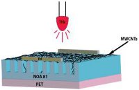 Significant THz Applications: Medical Imaging - Cancer detection; Explosive detection; Astronomy; Non invasive - Security scanning in Airports; Large-scale integrated circuit testing; Information and communication technology wireless -40 Gbit/s; Weather monitoring. CHM Test Bed Results: Developed a new method for the production of low cost, sensitive, room temperature THz detectors on a R2R platform; Only suspended CNT devices registered THz detection; Detection sensitive to bias voltage and thickness of MWNT films; Fabrication processes are completely adaptable to R2R platform; Work envisions a potential merging of nanoimprint technologies and THz technologies for the scale up and advancement of emerging THz applications.
Materials and Processes for Flexible Devices and Electronics
 The symposium was attended by more than 150 participants from academia, government and industry, with 50 companies and 10 academic institutions represented. Topics included: Nanoarchitecture control for photovoltaics (PVs); Material design & device engineering for polymer PVs; Roll-to-roll (R2R) nanomanufacturing processes for displays & Photovoltaics; Printed & hybrid flexible electronics; Polymeric semiconductors for printed opto-electronics; Conformal electronics for the human body; R2R nanoimprint lithography; Advances in electrophoretic display technology; Integration of high performance electronics into flexible packaging.
UMass Amherst Center for Personalized Health Monitoring and Biometric Sensors Utilizes CHM Process Platforms
 The CPHM will include the $25,000,000 Center for Advanced Roll-to-Roll Manufacturing for the Life and Nano Sciences, an open access facility that will deploy leading edge technology and pilot tools for sensor systems, packaging and associated flexible electronics platforms and enhance University – Industry partnerships. This Center is built upon and has been enabled by advances in the CHM.
SciTech Café
 The PIs founded SciTech Café, which held its inaugural event in September 2012, and meets about monthly at a local restaurant. PI Aidala led the June event, introducing nanotechnology to the audience of over one hundred people.
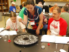
Nanotechnology Training for K12 Science Teachers at the NSEC Center for Hierarchical Manufacturing
 The CHM conducted its seventh annual Nanotechnology Summer Institute for K12 science teachers at UMass Amherst, July 8-12, 2013. Twenty-seven teachers learned from an array of nanotechnology modules with many hands-on activities for the classroom, including module on self assembly, constructing an model atomic for microscope, creating a nanofilm, and more. http://www.umassk12.net/nano/
“Informatics for Nanomanufacturing” Workshop: October 15, 2013
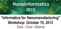 The National Nanomanufacturing Network (NNN) coordinated a workshop convening participants from industry, academia and government to discuss the utilization of informatics in nanomanufacturing. This workshop helped to identify compelling data and tools, factors that make data useful and searchable, strategies for sharing data, mapping terminologies and ontologies and mechanisms for strong industry involvement in the nanoinformatics effort. Held in Philadephia PA at the University of Pennsylvania.
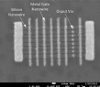
Roll-to-Roll Fabrication of Flexible Low-operating Voltage Organic FETs using Solution-based Hybrid High-K Dielectrics
 Organic field effect transistors (OFETs) are key for flexible, lightweight, and inexpensive electronic devices. Low-voltage operation of OFETs is necessary for many practical applications and all solution-based, low-temperature processes are desirable as they provide a significant cost advantages for scaling to large area roll-to-roll fabrication processes. To meet these challenges the CHM has developed solution-based high-k dielectric coatings consisting of zirconia (ZrO2) nanoparticles in a polymer composite.
NNN/InterNano Accomplishments and Goals 2011-2016
 Going Forward: National Roadmap, Federated Databases, Nanomanufacturing Standards, Workforce Training
Formation of Pre-Competitive R2R Research Consortium
 Launched in 2011 as part of the Center for University of Massachusetts / Industry Research on Polymers (CUMIRP), the precompetitive industry research consortium for Roll-to-Roll Processing designated as Cluster R has grown to seven industry members. Member meetings were held in the spring and fall and a dedicated “Member Only” website for disseminating reports and receiving member input was set-up.

Reconfigurable Nanowire Fabric for Computation: Simulations and Experimental Prototyping
 The Reconfigurable Nanowire Fabric is targeted as a scalable alternative to CMOS FPGAs. Logic and memory functionalities can be mapped on to programmable nanowire arrays with reconfigurable cross-nanowire field effect transistor (xnwFETs) crosspoints. Design choices across device, circuit and architecture level are geared towards reducing manufacturing requirements – junctionless xnwFET devices eliminate the need for stringent control of doping profile, regular arrays with limited customization imply mitigated overlay precision requirements, novel circuit styles eliminate the need for arbitrary fine-grain sizing, doping and routing. Furthermore, this fabric uses a fine-grain device-level reconfiguration approach that could have an order-of-magnitude area/power/performance improvement vs. conventional schemes.
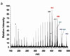
Nanoparticle-Based Anticounterfeiting
 We have developed an anti-counterfeiting strategy based on the ionization of ligands from gold nanoparticles. In practice, the particles were inkjet printed onto surfaces, and the “mass barcodes” arising from different ligands was read off using laser desorption mass spectrometry (LDI-MS). This method provides rapid and efficient authentication of materials, with applications in pharmaceuticals, currency, and other areas where counterfeiting is common.
Nanotechnology Training for K12 Science Teachers at the NSEC Center for Hierarchical Manufacturing
 The CHM conducted its sixth annual Nanotechnology Summer Institute for K12 science teachers at UMass Amherst, July 9-13, 2012. Twenty-seven teachers learned from an array of nanotechnology modules with many hands-on activities for the classroom, including a lesson on self assembly. A second Institute was added this year on July 17-19, 2012 for twenty-three teachers in Albany, NY. The teachers used these modules to develop curriculum plans that meet their particular teaching needs and satisfy state standards. http://www.umassk12.net/nano/
Multiplexed Imaging of Nanoparticles in Tissues
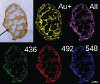 To more fully understand the biodistributions and potential toxicity of nanoparticles (NPs) that are released into the environment, it is essential to monitor the spatial distributions of NPs in vivo. To this end CHM scientists have developed an approach based on laser desorption/ionization mass spectrometry (LDI-MS) to image NPs in tissues. Because MS is used as the readout for this imaging approach, multiple NPs can be imaged simultaneously, which facilitates the side-by-side comparison of different NP types. Results indicate that NPs can remain intact in animals and that biodistribution information can be directly obtained.
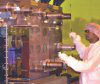
Roll-to-Roll Nanoimprint Test Bed
 The CHM has initiated a new roll-to-roll system-level test bed program to facilitate the development of a manufacturing platform for fabrication of low-cost, large-area nano-materials and devices using roll-to-roll processing technology. This roll-to-roll process test bed was developed to address the challenge of fabricating nanostructured thin films on a high-speed, high-reliability platform. Moving forward, this test bed will enable low-cost commercialization of nanotechnology in applications ranging water purification & filtration, batteries and thin film organic-based photovoltaics. The center accepted delivery of the first custom roll-to-roll nanoimprint lithography (R2RNIL) tool in June 2011. Center researchers are now routinely printing sub-200 nm features in a continuous web process. Center researchers are currently developing new materials and processes to enable printing of features to the ten’s of nanometers. Understanding flow and rheological properties is critical to the mission. Real-time inspection and metrology capabilities are being developed for the new tools.
Floating Gate Memory via Additive Driven Assembly: Opportunities for Device Fabrication using Solution Processing and Roll-to-Roll Manufacturing
 We have used additive driven self-assembly to create the active device layer for floating gate memory. This approach, which allows for very high loadings of 2 nm gold nanoparticles in a polystyrene-block-poly(vinyl pyridine) block copolymer, offers theoretical storage capacities competitive with current flash memory devices. To achieve high storage densities in devices, device level patterning at micron and smaller length scales is required. We are currently pursuing the device patterning via roll-to-roll (R2R) nanoimprint lithography. These technologies will enable the production of memory and other devices using low cost, sustainable, nanomanufacturing.
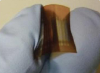
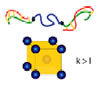
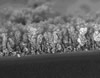
Nanoimprinting on Impregnated Fabric Substrates
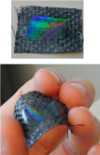 The Carter and Crosby research groups have collaborated to develop new methods to overcome existing challenges in the use of nanoimprinting patterning on flexible substrates in a roll-to-roll configuration. One of the major challenges is the delamination of imprinted materials from flexible substrates, such as PET films. To overcome delamination, we have recently proposed and demonstrated the use of woven substrates, rather than films, to allow mechanical interlocking to help in preventing unwanted delamination. In our process, we impregnate a woven fabric, with a curable formulation, which can subsequently be imprinted with a nanostructured pattern (top schematic). Our initial results (bottom images) are encouraging, and we are currently determining the material and spatial limits of this approach, as well as the mechanical properties of imprinted samples.
Towards High-Rate Nano-Manufacturing of Gold Nanoparticle Lines
 We prepared lines from Au NPs, using advances in flow-coating methodology, and measured their conductivity on inter-digitated electrodes. These line arrays exhibited an ohmic, linear current-voltage response similar to conductive material. The conductivity of the Au NP lines, measured from top contact configuration (electrode on Au NP lines) is 4 orders of magnitude higher than reported values of Langmuir monolayers of Au NPs. The performance and reproducibility of these lines were confirmed by control experiments and fabrication-characterization of numerous Au NP line arrays. We also found that these lines can be deposited on non-uniform substrates (Au NP lines on electrode), resulting in shape-conforming conductive paths.
Thermoreflectance Microscopy: Metrology for Optoelectronic Devices
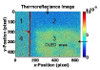 The luminance and lifetime of OLEDs decrease dramatically with increased device operating temperature due to self-heating; this problem is particularly severe in OLEDs operated at high-brightness conditions. For stand-alone OLEDs, self-heating leads to measured rises in average temperatures of up to 60°C, with local temperature rises of up to 200°C, reducing lifetime by 20x or more. Thermoreflectance imaging, can be used through glass to characterize the thermal performance of an operating OLED and inspect the temperature profile spatially to help increasing the lifetime of high brightness OLEDs with better thermal design.
A Natural Route to Nanowires and Energy Storage
 Organic electronics is a burgeoning area, with a growing range of applications. This new research – in which nanowires are grown naturally rather then synthesized chemically – may provide new methods for biologically-produced or biologically-inspired materials for sustainable nanomanu-facturing. Pilin nanofilaments (pili) — known now as “microbial nanowires” — are a class of fibrous proteins found in the sediment bacteria Geobacter. Temperature studies find metallic characteristics. The conductivity can be modulated by doping or by using an applied voltage in an electrochemical transistor configuration, showing the potential for device applications, including supercapacitors for energy storage.
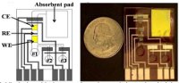
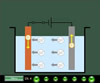
Microfluidic Sensors for Resource-limited Areas
 An ideal point-of-care device would incorporate the simplicity and reliability of a lateral flow assay with a microfluidic device. Our system consists of self-priming microfluidics with sealed conjugate pads of reagent delivery and an absorbent pad for additional fluid draw. Using poly (methyl methacrylate) (PMMA) as a substrate, we have developed a single-step surface modification method which allows strong capillary flow within a sealed microchannel. Conjugate pads within the device held trapped complex consisting of the magnetic beads and nucleic-acid-probe-conjugated horseradish peroxidase (HRP). Magnetic beads were released when sample entered the chamber and hybridized with the complex. The complex was immobilized over a magnet while a luminol co-reactant stream containing H2O2 was merged with the channel. A plate reader was able to quantify the chemiluminescence signal. This new format of biosensor will allow for a smaller and more sensitive biosensor, as well as commercial-scale manufacturing and low materials cost.
Quantum Dot Stability in Cells is Size Dependent
 Quantum dots (QDs) are highly fluorescent and photostable, making them excellent tools for imaging. When using these QDs in cells and animals, however, intracellular biothiols can degrade the QD monolayer compromising function. CHM scientists have developed a label-free method to quantify the intracellular stability of monolayers on QD surfaces that couples laser desorption/ionization mass spectrometry (LDI-MS) with inductively coupled plasma mass spectrometry (ICP-MS). Using this new approach they have demonstrated that QD monolayer stability is correlated with both QD particle size and monolayer structure, with proper choice of both particle size and ligand structure required for intracellular stability.
National Nanomanufacturing Network Events
 Nanoinformatics 2011 brought together informatics experts, nanotechnology researchers, and other stakeholders and potential contributors to advance Nanoinformatics 2020 Roadmap goals. The workshop will set a clear path for Nanoinformatics participants through the presentation of projects and research, open discussions, and strategic planning sessions. The Nanomanufacturing Summit 2011 – showcased emerging areas of nanomanufacturing and commercialization of nanotechnology-enabled products by leaders in the field of nanomanufacturing.
Nanotechnology Training for K12 Science Teachers at the NSEC Center for Hierarchical Manufacturing
 The CHM conducted its fifth annual Nanotechnology Summer Institute for K12 science teachers at UMass Amherst, July 11-15, 2011. Twenty-seven teachers learned from 10 nanotechnology modules with many hands-on activities for the classroom, including a lesson on self assembly. The teachers used these modules to develop curriculum plans that meet their particular teaching needs and satisfy state standards. http://www.umassk12.net/nano/
Bringing Bottom-Up to Roll-to-Roll
 The CHM is developing process tools and materials sets to enable the self-assembly of ordered hybrid materials and imprinting of nanostructured features on roll-to-roll platform for low cost nanomanufacturing of devices. Applications include energy generation and storage, separations, sensors and flexible electronics
Low-Cost Test Strips for Microbe Detection
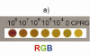 Bacterial contamination of drinking water is an important issue both domestically and in developing nations. CHM researchers have developed a test-strip based sensor platform capable of detecting bacteria. This strategy uses nanoparticle-enzyme complexes to generate colorimetric responses that provide visual quantification of bacteria levels. Pilot studies using microspotting have demonstrated excellent sensitivity. Porting of this methodology to inkjet processing has been promising, providing a potential pathway to manufacturing low-cost answers to the world-wide issue of bacterial contamination.
Nanoparticle Surface Properties Dictate Uptake and Toxicity in Fish
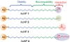 Very little is currently understood regarding the role of surface properties in determining in vivo behavior of nanomaterials. In studies using Medaka fish, we have found that hydrophilic NPs 1-3 are found predominantly in the gills and intestines and are cleared from the fish over time. Hydrophobic particle 4, however, is rapidly taken up and distrubuted throughout the fish with toxic consequences. These studies show that surface properties are key determinants of the environmental impact of nanomaterials.
CHM Test Bed: Roll-to-Roll Process Facility
 The CHM has established a unique roll-to-roll (R2R) process facility that will serve as a test bed for scaleable, cost-effective nanomanufacturing of functional, nanostructured materials and devices. This facility includes new process tools for UV-assisted R2R nanoimprint lithography and R2R coating for nanostructured hybrid materials. The tools were developed in cooperation with our industry partners and will be delivered in Q2 and Q3 of 2011. The CHM further launched a dedicated Industry Advisory Board (IAB) to support and collaborate on the R2R test bed. The IAB includes 14 members from a broad spectrum of companies. Demonstration projects will include polymer batteries, membranes for nanoseparations, flexible photovoltaics and flexible electronics. New collaborations with MIT, Rice and the Center for Nanoscale Science and Technology at NIST bring additional expertise in manufacturing science and metrology to the effort.
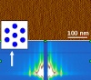
Nano-Engineered Magneto-Electronic Materials Made by Self-Assembly
 CHM researchers and NIST collaborators used self-assembly to create a new type of metamaterial in which the electronic properties are tuned by the periodic spacing and magnetic moment of an array of ferromagnetic nanoparticles atop a metal film. The significance of this "artificial Kondo lattice" is the engineering of electronic functionality through nanoscale structure--an important new step towards materials by design. Physical Review B 83, 014408 (2011)
Nanotechnology Training for K12 Science Teachers at the NSEC Center for Hierarchical Manufacturing
 The CHM conducted its fourth annual Nanotechnology Summer Institute for K12 science teachers at UMass Amherst, June 28-July 2, 2010. 30 teachers learned nine nanotechnology modules with hands-on activities for the classroom. As part of the week's activities, the teachers used these modules to develop curriculum plans that meet their particular teaching needs and satisfy state standards. http://www.umassk12.net/nano/
Nanoinformatics 2010
 Nanoinformatics 2010 is a collaborative roadmapping and workshop project at which informatics experts, nanotechnology researchers, and other stakeholders and potential contributors will jointly develop a roadmap for the area of nanoinformatics. http://nanotechinformatics.org/
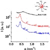
Macroscopic 10 Terabit/in2 Arrays from Block Copolymers
 A collaboration between UMass and UC Berkeley researchers funded by the NSF and DOE has led to a breakthrough in the areal density of templates derived from block copolymers (BCPs) having orientational registry over macroscopic distances. The facets on a reconstructed single crystal surface were used to guide and direct the self-assembly of BCPs having 3 nm cylindrical domains over arbitrarily large surfaces. Grazing incidence x-ray scattering (GISAXS) quantitatively demonstrated the perfection in the orientational order and the quasi-crystalline long-range lateral order of the arrays. The unprecedented small size of the domains could revolutionize bit patterned storage media and yield capacities over 10.5 Tbit/in.2
Nanoparticle Driven Assembly of Ordered Polymer-Nanoparticle Hybrid Materials
 Ordered polymer-nanoparticle (NP) hybrid materials are at the heart of many nanotechnology enabled applications in energy conversion, optical, magnetic and photonic devices, separations and sensors. The addition of NPs to block copolymer templates however often compromises order at modest loadings. CHM research has demonstrated that the use of strong specific interactions between the NP and one segment of the polymer can induce order in otherwise disordered materials at particle loadings of more than 30%.
Nanoscale Patterns Made by Hierarchical Self-Assembly
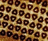 CHM researchers demonstrated hierarchical patterning techniques that combine electron-beam lithography and block copolymer self-assembly for patterned data storage media. This work investigates block copolymer self-assembly under geometric constraints to produce arrays with long-range order or alternatively a precise number of elements. Enables patterned magnetic media for binary or multibit applications.
Unique “Chemical Nose” Sensors for Cancer Cell Detection
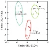 Building off fundamental studies on the interactions between nanoparticles with proteins and cells, CHM researchers have developed unique “chemical nose” sensors for cells and serum. Pilot studies have indicated the utility of these sensors in the rapid and efficient identification of healthy, cancerous, and metastatic cells for cancer diagnosis. Similar approaches are now being explored to modify this approach for enzyme-nanoparticle sensors for bacterial contamination that can be implemented in a mass-producible and cost-effective test strip format.
Nanotechnology Training for K12 Science Teachers
 The CHM conducted the third annual Nanotechnology Summer Institute for K12 science teachers at UMass Amherst, July 20-24, 2009. 32 teachers learned nine nanotechnology modules with hands-on activities for the classroom. As part of the week's activities, the teachers used these modules to develop curriculum plans that meet their particular teaching nees and satisfy state and federal standards. http://www.umassk12.net/nano/2009summer/
Inexpensive Templates for Nanostructure Fabrication
 Researchers at the University of Massachusetts Amherst have discovered a new method of formulating common polymers for industrially generating templates used in precision nanomanufacturing. The researchers found that blending commercially-available tri-block copolymer surfactants with commodity polymers that selectively associate with one of the blocks can yield bulk quantities of polymeric templates with well-ordered periodic nanostructures.
Nanoparticle-Polymer "Chemical Nose" Sensors
 A team at the University of Massachusetts Amherst has created a sensor array to detect, identify, and quantify protein targets. The polymer fluorescence is quenched by gold nanoparticles: the presence of proteins disrupts the nanoparticle-polymer interaction, producing distinct fluorescence response patterns. These patterns are highly repeatable and are characteristic for individual proteins at nanoscale concentrations. Quantitative analysis was used to identify 52 unknown proteins with an accuracy of 94%, demonstrating that nanomaterial-based protein detectors are potentially feasible for “chemical nose”applications in medical diagnostics.
Beyond-Binary: Nanomagnet Clusters for Data Storage
 Using ultrahigh resolution electron beam lithography, a team led by Prof. Mark Tuominen at the University of Massachusetts Amherst has fabricated clusters containing a well-defined number of interacting cobalt nanomagnets. With multiple stable states, the clusters can be used to encode and store data beyond the limits of conventional binary storage. This method may serve as a way to pack more data into a fixed area in hard drive and memory applications. The researchers are now attempting to scale-up the fabrication of these multistate nanomagnets to larger areas by using hierarchical patterning methods on diblock copolymer films.
Network Established to Spur U.S. Nanomanufacturing
 The NSF Center for Hierarchical Manufacturing (CHM) at the University of Massachusetts Amherst, in teamwork with other academic, government and industrial programs devoted to the new technology of nanomanufacturing, has established an R&D network and cyber-clearinghouse for this industrially-important field. The National Nanomanufacturing Network (NNN) will sponsor networking, collaborative events, education and information exchange for America’s nanomanufacturing research and technology community. Its digital library, InterNano, of nanomanufacturing technical information, resource directories and NNN events can be found at http://www.internano.org.
Scientists Develop Educational Modules on Nanotechnology
 A team at the Center for Hierarchical Manufacturing at the University of Massachusetts Amherst has developed a systematic approach for producing repurposable educational videos that utilize a combination of live video and 3D animation to convey complex concepts in nanotechnology. The first group of videos were produced and evaluated by teachers and students in K-12, community college and university learning environments. The repurposable content enables adaptation for various audience levels, instructional approaches, and languages.
Multiplexed Screening of Cellular Uptake of Gold Nanoparticles Using Laser Desorption/Ionization Mass Spectrometry (LDI-MS)
 With the increased production of nanotechnology-related products and the inevitable release of some of these materials into the environment, nanoparticle uptake by living organisms in the environment is an area of growing interest. CHM scientists have developed a rapid and efficient means for tracking cellular uptake of functionalized gold nanoparticles using the gold core to greatly facilitate ligand ionization. These ligands act as mass barcodes that allow many particles to be followed simultaneously. This method will provide direct access to bio-distribution data: in vivo studies using fish (Japanese medaka) are underway.
Binary Semiconductor Nanowires Through Templated Electrodeposition
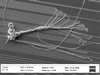 Nanoscale well-defined heterojunction semiconductor structures are desired for efficient photovoltaic devices. CHM Researchers have created nanowires of cadmium selenide (CdSe) on indium tin oxide (ITO) substrate using a simple electrochemical deposition process and polymer templates created by nanoimprint lithography. The wires are ~400 nm wide and span length of the substrate (1 cm x 1 cm).
Spray-on Crystalline Metal Oxide Semiconductor Nanostructures for Low Cost PVs and H2 Generation
 High surface area, nanostructured, crystalline metal oxide films are of interest for solar energy conversion via photovolatic cells and H2 generation via photocatalytic water splitting. Researchers at the CHM in partnership with Inframat Corporation have developed a new ultra-low cost technology for spray on nanodendritic films of TiO2, ZnO and other metal oxides.
InterNano - The Nanomanufacturing Information Clearinghouse and Web Portal to the National Nanomanufacturing Network (NNN)
 InterNano.org officially launched in 2008 to support the nanomanufacturing research, development and education community as cyberinfrastructure that collects, organizes and disseminates information in the nanomanufacturing domain. The website serves as the web home of the NNN and provides a directory of experts and centers, a process database, a taxonomy, highlights, reports, reviews, news, events and other features.
K12 Education
 The Center for Hierarchical Manufacturing (CHM) provided a week-long nanoscience education workshop to K12 teachers from across the nation. These 29 teachers received training in a range of hands-on activities, discussions and video-based curriculum materials suitable for classroom implementation. The CHM developed new learning modules suitable for K12 education. These open-source curriculum materials, which are rich in video and 3D animation, have been designed so that they are easily edited and repurposable for other audiences in other learning environments. Modules are accessible from the center's website: www.umass.edu/chm